



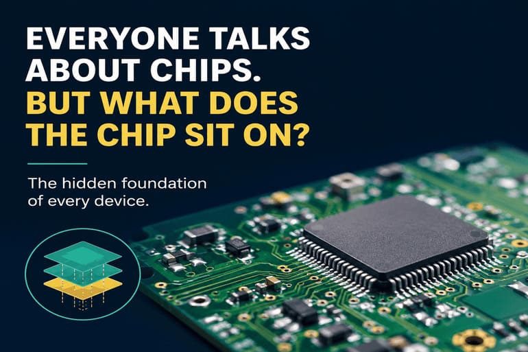
The semiconductor has become the celebrity of India’s electronics ambitions. Governments are talking about semiconductor fabs, companies are announcing investments, policymakers are discussing chip design and packaging, and the word “semiconductor” has become almost synonymous with India’s ambition to become a serious electronics manufacturing power. That attention is understandable. The chip is the brain of an electronic device, and whoever controls advanced semiconductor manufacturing holds an important position in the technology value chain.
But there is another piece of technology sitting quietly underneath almost every chip, and it rarely receives the same attention. It does not have the glamour of a semiconductor fab or the strategic importance attached to a chip. Yet without it, the chip cannot do much on its own. That component is the printed circuit board, better known as the PCB.
Every time we use a smartphone, laptop, television remote, automobile or countless other electronic products, we are relying on PCBs to make the electronics inside them work together. A chip needs something to sit on, something to connect it to other components and something to carry electrical signals from one part of the device to another. The PCB performs all of these functions. It is the physical and electrical platform on which an electronic system comes together. And that makes the PCB far more important to India’s electronics ambitions than its relatively low profile might suggest.
The Circuit Board Is Not Really a Board Anymore
Most people probably imagine a PCB as a flat green board covered with thin copper lines. That image is not entirely wrong, but it tells only a small part of the story. The simplest way to understand what a PCB actually does is to imagine the electrical system inside a building. There is a main control panel, electrical devices distributed throughout the building and wires connecting everything together. Electricity and signals have to travel from one point to another in a controlled manner.
A PCB performs essentially the same job, except that the entire electrical network is compressed into an incredibly small physical space. The wires become copper tracks etched onto the surface and inside the board. LEDs, sensors, memory devices and other electronic components take the place of the electrical devices in the building, while semiconductor chips become some of the most important elements connected to that network. What would require metres of wiring in a building can be engineered into a circuit board that fits inside a device small enough to hold in the palm of your hand.
The really fascinating part begins when the electronics become more sophisticated. A simple television remote might use a relatively straightforward single-layer PCB, while other products may use two layers, with electrical tracks on both sides. As the number of components increases and the available physical space decreases, manufacturers can add more layers. Automotive electronics can use multi-layer boards with several layers of electrical connectivity, while advanced consumer devices can require dozens of layers.
This is where the building analogy becomes particularly useful. A modern smartphone PCB can be around one millimetre thick, roughly comparable to the thickness of a credit card, yet it can contain dozens of layers within that extremely small space. Each layer can carry its own copper tracks and electrical connections, while tiny plated holes connect one layer to another. In effect, these holes function like staircases or elevators connecting different floors of a miniature building.
So when we hold a smartphone, we are not simply holding a flat board with some wires printed onto it. We are holding a highly compressed, three-dimensional electrical structure in which dozens of layers have been engineered to operate together within approximately a millimetre of thickness. The fact that we rarely think about this is perhaps the best evidence of how far electronics manufacturing has evolved.
Also Read: India’s Component Boom: 106 ECMS Projects set to reshape Electronics Supply Chain
Where Half a Hair’s Width Can Decide Success or Failure
The complexity of a multi-layer PCB becomes even clearer when we look at how it is manufactured. The different inner layers are produced separately and then stacked together before being pressed into a single structure. Once the layers have been pressed together, however, the manufacturer can no longer simply look inside the board and check whether everything is perfectly aligned. The inner layers have effectively disappeared from view.
The next stages therefore depend on extraordinary levels of manufacturing precision. Holes have to be drilled through the stack at exactly the right locations so that they connect the intended electrical pathways between different layers. The copper tracks have to be created with precise dimensions, and the entire structure must remain stable throughout multiple manufacturing processes.
The level of precision required can be astonishing. A shift of around 50 microns during the pressing process can be enough to make an entire board unusable. Fifty microns is roughly half the thickness of a human hair. Consider what that means in practical terms. Manufacturers are taking dozens of layers, compressing them into a structure around a millimetre thick and expecting the electrical pathways on those different layers to line up with extraordinary accuracy. A deviation that is almost impossible to see with the naked eye can turn the entire product into scrap.
This is why PCB manufacturing should not be viewed simply as a business of producing boards. It is a precision manufacturing discipline that combines materials, chemistry, electrical engineering, machinery, process control and human experience. As the industry moves towards finer tracks and higher-density boards, the margin for error becomes smaller still. Moving from something like a 150-micron track towards a 25-micron track is not merely a matter of making the same product smaller. It requires manufacturers to control the process at an entirely different level. And that brings us to a part of manufacturing that is often overlooked when countries talk about building factories.
The machines are important. But the people who know how to make those machines consistently produce the right result may be even more important.
Also Read: The Next Energy Frontier: Abinash Sahoo on India’s Battery Ambition
The Manufacturing Knowledge You Cannot Buy From a Catalogue
A manufacturing manual can tell an engineer what a machine is supposed to do. It may specify temperatures, pressures, chemical concentrations, tolerances and process times. But manufacturing rarely behaves like a perfectly controlled textbook experiment. The same machine can produce different results under different conditions. Materials can behave differently from one batch to another. Environmental conditions can affect processes. A defect can appear even when every parameter appears to be within specification.
Someone who has spent years working on the factory floor often develops an instinct for these variations. They begin to understand which small changes matter, which problems are likely to appear later in the process and which seemingly minor deviation could become a major production failure. Much of that knowledge is difficult to capture in a manual or transfer through a classroom.
This accumulated experience is one of the invisible assets of an industrial ecosystem. It is also one reason why building a manufacturing industry takes time. You can import a machine tomorrow, but you cannot instantly recreate twenty years of manufacturing experience around that machine.
That distinction is particularly important for India because the country’s electronics ambitions are now moving into areas where manufacturing depth matters enormously.
India’s Electronics Opportunity: Building the Next Manufacturing Layer
India has built extraordinary capabilities in software and services, but physical electronics manufacturing has followed a very different trajectory. The country today has a large and growing electronics market, significant smartphone manufacturing activity and increasing policy support for domestic production. Semiconductor investments are also beginning to change the conversation around the country’s technological capabilities.
But an electronics ecosystem is not built around a single component. A semiconductor fab does not exist in isolation. Chips need packaging, substrates, PCBs, connectors, power systems, testing equipment and countless other components and processes before they become part of a finished electronic product. The strength of an electronics manufacturing ecosystem therefore depends on how many of these interconnected layers can develop together.
The PCB is particularly important because it sits directly in the middle of this ecosystem. It connects semiconductors to other components and provides the electrical architecture through which the entire system functions. It requires inputs from multiple industries, including copper, laminates, chemicals, manufacturing equipment and precision tooling. It also depends on engineers, technicians, designers, quality specialists and increasingly sophisticated automation systems.
This means India’s PCB challenge is not simply about encouraging companies to build more factories. It is about creating the ecosystem that allows those factories to become progressively more sophisticated.
India has to be able to manufacture increasingly dense boards, improve yields, reduce defects, develop local supply chains, strengthen testing capabilities and build the manufacturing knowledge required to compete at the highest levels. The objective should not simply be to produce more PCBs. It should be to steadily move up the technology curve.
India Was Not Always Behind
There is another reason the PCB story deserves closer attention. India’s current position should not be viewed as the inevitable result of being technologically incapable of manufacturing advanced electronics. India had a PCB manufacturing base as far back as the 1980s and was, in some respects, ahead of China at that time. The more important question is what happened afterwards.
China’s electronics manufacturing rise was not simply a story about cheaper production. Over time, manufacturing capability, engineering talent, suppliers, customers and technology began to accumulate around each other. As global electronics companies shifted significant portions of their production to China, engineers and technical knowledge moved along with the factories and orders. Manufacturing experience that had taken decades to accumulate elsewhere increasingly became part of China’s industrial ecosystem.
India’s economic priorities moved in another direction. The country’s success in information technology and services became one of its greatest economic strengths, but the physical manufacturing ecosystem did not expand at the same pace.
That history matters because it offers an important lesson for the present. India’s ambition to become a global electronics manufacturing hub is supported by a long-term process of capability building. A strong ecosystem takes shape through sustained production, investment, innovation, hands-on experimentation, and the lessons gained at every stage of growth.
The good news is that India now has an opportunity to build that capability with a much larger domestic market, stronger electronics demand and a government increasingly focused on manufacturing. But the country will need to think beyond the headline investment numbers.
Also Read: “Made in India” Isn’t Enough: From Wheels to Code, Priyank Rakholiya on Building the Indian EV
The Chip Cannot Become the Whole Semiconductor Story
India’s semiconductor ambitions are undoubtedly important. Building domestic capability in chip manufacturing, packaging and related technologies can strengthen the country’s technological resilience and create new industrial opportunities. But there is a danger in allowing the semiconductor conversation to become too narrowly focused on the chip itself.
A chip is one part of a much larger electronic system. The real test of India’s electronics manufacturing ambitions will be whether the country can build the ecosystem around the chip. Can it manufacture sophisticated PCBs? Can it develop reliable component supply chains? Can it produce advanced materials locally? Can it build precision manufacturing expertise? Can it develop engineers and technicians who understand the realities of high-volume electronics production? Can it create an environment where suppliers and customers grow together?
These questions may not generate the same headlines as a new semiconductor fab, but they will determine how deeply India participates in the electronics value chain. The PCB is an excellent illustration of this challenge because it looks deceptively simple from the outside. A board with copper tracks does not sound particularly revolutionary. Yet behind that board is an extraordinary combination of engineering, chemistry, materials science, precision manufacturing and accumulated human knowledge. The more advanced the electronics become, the more demanding that hidden infrastructure becomes.
The Invisible Foundation of India’s Electronics Future
Perhaps the most interesting thing about PCBs is that consumers almost never notice them. We notice the screen on our smartphone, the quality of its camera, the speed of its processor and the battery life. We notice the features and the design. We rarely think about the layers of copper and insulating material hidden inside the device that allow all those features to work together.
But perhaps it is time to look beneath the surface. India’s electronics ambitions will not be determined by one semiconductor fab, one smartphone factory or one large investment announcement. They will be determined by whether the country can develop the dense network of manufacturing capabilities that sits underneath the finished product.
The PCB is one of those foundational capabilities. It may not be the most visible component in an electronic device, but it is one of the most important. It carries signals, connects components and provides the physical architecture on which modern electronics are built. And as devices become thinner, faster and more powerful, the engineering demands placed on that architecture will only increase.
The real opportunity for India, therefore, is not simply to make more circuit boards. It is to develop the knowledge, precision and industrial ecosystem required to make increasingly sophisticated circuit boards consistently and competitively.
Everyone may be talking about chips today. But if India wants to build a complete electronics manufacturing ecosystem, it will have to pay much more attention to what the chip sits on.
Because sometimes the foundation tells you more about the strength of a building than the tallest floor ever could.

2 Comments
Pingback: GRSE inks MoU with Damen to build advanced dredgers
Pingback: OGP’s New SmartScope E18 for Precision Video Measurement