



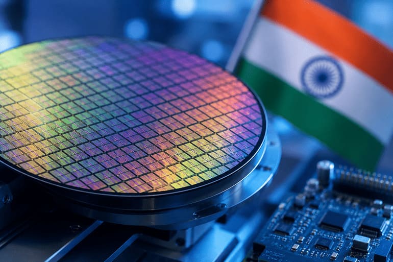
The most important decision in India’s semiconductor journey may not be how small a chip it can make, but which chips it should learn to make first. The global semiconductor race is increasingly measured in nanometres. The conversation around 3nm, 2nm and even smaller process technologies dominates headlines, particularly as Artificial Intelligence and High-Performance Computing push demand for ever more powerful chips. But for India, the immediate challenge is somewhat different. The country is still building the manufacturing capabilities, workforce and supply-chain ecosystem required to operate semiconductor fabrication at commercial scale. That raises a fundamental question: Does India need to compete at the leading edge immediately, or would mature semiconductor technologies provide a more practical route into manufacturing?
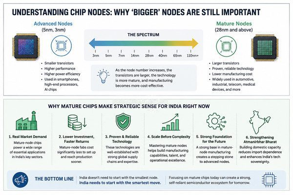
There is a strong case for the latter. Mature-node chips, broadly, including technologies such as 28nm and above may not attract the same attention as the newest processors, but they remain important across automobiles, industrial equipment, telecommunications, medical electronics, power management and other applications. India’s first major commercial fabrication plans also point in this direction. Tata Electronics’ planned semiconductor fab in Dholera, Gujarat, is designed for Analog and Logic IC production using 28nm to 110nm technologies, with planned capacity of 50,000 wafers per month.
That is not necessarily a compromise. It could be a sensible starting point for a country that needs to build manufacturing expertise before attempting to climb further up the technology ladder.
Also Read: Pace Digitek Scales Up Energy Storage With 300th BESS Container and 1.5 GWh Milestone
The Semiconductor Industry is much Bigger Than the Leading Edge
The fascination with leading-edge semiconductors can make it easy to overlook the enormous number of chips that do not require the latest process technology. A modern automobile, for example, depends on semiconductors for power management, sensing, control systems and communications. Industrial machinery, healthcare equipment, telecom infrastructure and consumer electronics similarly use a wide variety of chips with different performance and reliability requirements.
For many of these applications, the smallest possible transistor is not necessarily the most important consideration. Cost, reliability, availability, long product cycles and supply-chain security can be equally important. That makes mature technologies commercially significant even in an industry that is constantly talking about smaller nodes.
For India, this creates an opportunity to build manufacturing strength around technologies that already serve a broad industrial market rather than attempting to replicate the world’s most advanced fabs from the outset. The Dholera project is particularly relevant in this context. Tata Electronics says its planned fab, being developed with Taiwan’s Powerchip Semiconductor Manufacturing Corporation will produce analog and logic integrated circuits across the 28nm-110nm range, with applications including power-management ICs, display drivers and microcontrollers.
The broader point is simple: semiconductor manufacturing does not have to begin with the world’s smallest node to become strategically valuable.
India’s First Challenge is to Build Manufacturing Capability
A semiconductor fab is not simply a building filled with expensive equipment. It is an extremely complex manufacturing environment that depends on process engineering, yield management, equipment maintenance, ultra-clean production conditions, specialized materials and gases, reliable utilities, testing, packaging and a highly trained workforce.
India does have semiconductor manufacturing experience. Semiconductor Laboratory in Mohali has operated an 8-inch 180nm CMOS fabrication line, giving the country a foundation of process and research expertise. But the scale and depth of India’s commercial semiconductor manufacturing ecosystem remain very different from those of the established global production centres.
That distinction matters because India’s first generation of commercial fabs will have to do more than produce chips. They will have to create an ecosystem around them. Engineers will need experience operating high-volume fabrication facilities. Suppliers will need to develop around the plants. Packaging and testing businesses will need to grow alongside wafer fabrication. Customers will have to qualify chips produced in India.
Over time, that experience can become one of the industry’s most valuable assets. Manufacturing knowledge is built through years of operating facilities, solving process problems, improving yields and developing relationships across the supply chain. This is why mature-node manufacturing can be viewed as capability building rather than technological retreat. The objective is to establish a manufacturing base, develop the ecosystem and create a platform from which more advanced technologies can eventually be pursued.
Also Read: ARC Informatique Launches PcVue 17 with AI, Energy Optimization and IEC 62443 Cybersecurity Features
The Economics Favour a Measured Approach
There is also a straightforward financial argument. Semiconductor fabrication is one of the most capital-intensive areas of manufacturing, while demand can move sharply through industry cycles. Governments around the world have therefore intervened with incentives designed to attract fabs and strengthen domestic supply chains.
India’s original Semicon India Programme carries an outlay of ₹76,000 crores, with the India Semiconductor Mission framework providing substantial fiscal support for semiconductor manufacturing and related activities. The policy push has subsequently broadened. Semicon 2.0 is intended to build a more comprehensive semiconductor ecosystem, with emphasis not only on fabrication and packaging but also on semiconductor design, manufacturing equipment, materials, research, talent and supply-chain resilience.
The logic is important. Public support can help make large semiconductor investments financially viable, but the longer-term value lies in what that support helps create around the factories. If investment contributes to the development of suppliers, engineers, design companies, equipment expertise and packaging infrastructure, the economic benefit can extend well beyond the life of an individual incentive. In that sense, the subsidy is not simply about building capacity. It is about using capital support to build an industry.
India Already has a Large Market Waiting for Chips
The strongest argument for building semiconductor manufacturing in India may ultimately be the size of the market itself. Government estimates put India’s semiconductor market at approximately $45-50 billion in 2024-25, with the market expected to reach $100-110 billion by 2030. The expansion is being driven by electronics manufacturing as well as demand from sectors such as automobiles, telecommunications, computing and other technology-intensive industries.
That creates a valuable starting point. India does not have to depend exclusively on exports to build an initial customer base. There is already a domestic ecosystem of electronics manufacturers and technology companies that need semiconductors. As electronics production increases, demand for chips should rise with it. That does not mean every chip consumed in India needs to be manufactured domestically. It does mean Indian fabs can potentially operate within a substantial local market while developing global customers.
This is where mature-node manufacturing becomes particularly relevant. A significant amount of industrial demand does not require leading-edge technology. If Indian companies can produce those chips reliably and competitively, they can address a large market without having to begin with the most expensive and technically demanding manufacturing processes.
The Tata Electronics Project Offers a Useful Model
The Dholera fab offers one of the clearest examples of what this strategy could look like. Tata Electronics says the planned facility will have a capacity of 50,000 wafers per month, with production spanning 28nm to 110nm technologies. The company has positioned the facility around analog and logic ICs and applications across multiple industries.
The significance of such a project goes beyond the number of wafers it may eventually produce. A facility of this scale creates demand for engineers, equipment servicing, specialized materials, logistics, testing and packaging. It also establishes relationships between Indian manufacturing and global semiconductor technology providers.
In other words, the fab can become an anchor for a broader industrial cluster. That could ultimately be more valuable than simply having one facility capable of producing a technically advanced chip.
Also Read: Vecros and JetCore AI Advance Autonomous Drones and Robotics With AI-Powered Technology
India should not confuse Advanced Chip Design with Advanced Chip Manufacturing
India also has another advantage that should not be underestimated: its semiconductor design talent. The government has been supporting semiconductor design startups through the Design Linked Incentive framework, while giving companies access to advanced electronic-design automation tools and encouraging chip tape-outs. By 2026, the government’s semiconductor programme had already created a pipeline of supported design projects alongside its manufacturing initiatives.
This is an area where India can continue to pursue advanced technologies even while its manufacturing base begins with more mature nodes. That distinction is important. Designing a 3nm chip and manufacturing a 3nm chip are not the same achievement. India can build advanced design capabilities while developing manufacturing expertise on mature processes. In fact, the two could eventually reinforce each other. Indian designers could gain better access to domestic manufacturing, while fabs could gain customers from an expanding domestic design ecosystem.
The strategic objective, therefore, should not be to choose between advanced design and mature manufacturing. India can pursue both, but it does not need to develop them at exactly the same pace.
The Global Subsidy Race is really a Supply-Chain Race
India’s approach also needs to be understood in the context of what is happening elsewhere. The United States, Europe and several Asian economies have used government incentives to attract semiconductor investment and reduce supply-chain dependence. The reason is straightforward: Semiconductors have become critical inputs for Automobiles, Defence Systems, Telecommunications, Computing and Artificial Intelligence.
The United States, for example, has created a major federal semiconductor incentive programme under the CHIPS Act, while Europe has developed its own Chips Act framework to strengthen manufacturing capacity and supply-chain resilience. The broader lesson is that governments increasingly view semiconductor production as strategic infrastructure rather than ordinary manufacturing.
India is entering this competition at a time when companies are also looking for greater geographic diversification. That creates an opportunity. India does not need to replace Taiwan, nor does it need to match China’s manufacturing scale overnight. Its more realistic objective is to become a dependable additional location in the global semiconductor supply chain. Mature-node manufacturing could provide a realistic starting point for that ambition.
Mature nodes are not an easy option. There is a danger, however, in making the mature-node argument sound too simple. A 28nm fab is still an extraordinarily sophisticated industrial facility. Lower technological complexity compared with a 2nm fab does not mean low complexity. Yield, uptime, quality control, process stability and customer qualification remain difficult.
India will still have to build deeper skills, strengthen its supplier ecosystem and develop operating experience. That is why the success of the semiconductor programme should not be judged only by the number of projects approved or the value of investment announced.
What Will Determine Whether India’s Semiconductor Bet Succeeds?
Some of the key indicators to watch will be:
- Commercial production: Can the new semiconductor facilities move into stable, consistent production at scale?
- Manufacturing efficiency: Can Indian fabs achieve competitive yields, quality and production efficiency?
- Customer adoption: Can the companies secure long-term customers in India and overseas and become part of global supply chains?
- Domestic supplier ecosystem: Can Indian companies increasingly provide the materials, equipment, services and other inputs required by semiconductor manufacturers?
- Talent and expertise: Can India build and retain enough skilled process engineers, technicians and semiconductor specialists to support the industry over the long term?
- Financial sustainability: Can semiconductor businesses build commercially competitive and increasingly self-sustaining operations as the industry matures?
These measures will ultimately tell us much more about the success of India’s semiconductor programme than the number of announcements alone.
The Real Value of the Subsidy Should be What Remains After it Ends
Government support can help make a semiconductor project financially viable. But the ultimate objective should be to use that support to create capabilities that remain long after the subsidy itself has been spent. That means experienced engineers, trained technicians, domestic suppliers, manufacturing know-how, intellectual property, customer relationships and research capabilities.
This is where the broader direction of Semicon 2.0 becomes significant. Its ecosystem approach recognizes that fabs are only one part of the semiconductor value chain. Equipment, materials, design, research, packaging and skilled people are equally important to creating a functioning industry.
If India gets those pieces moving together, mature-node manufacturing could become more than an entry point. It could become the foundation of a much larger semiconductor ecosystem.
Mature Nodes Could Lay the Groundwork for India’s Advanced Semiconductor Ambitions
There is nothing wrong with India aspiring to advanced semiconductor technologies. It should continue developing advanced chip-design capabilities and should ultimately aim to move higher up the manufacturing technology curve. But industrial strategy should not be judged by how impressive the headline sounds.
A 3nm fab would certainly attract attention. But an Indian fab that reliably produces millions of chips, meets international quality standards, develops a domestic supplier base and earns repeat orders from global customers may be a much more meaningful measure of industrial progress.
That is why mature chips deserve a closer look. They offer India access to a broad range of applications, a large domestic market and an opportunity to develop the operational capabilities that semiconductor manufacturing demands. They also give the country time to build an ecosystem around fabrication rather than attempting to solve every part of the semiconductor challenge simultaneously.
The goal should not be to choose mature chips instead of advanced chips forever. The goal should be to decide what India needs to master first. If the country can become highly capable at manufacturing mature-node semiconductors, build a reliable supply chain around those facilities and develop a strong domestic design ecosystem alongside them, the move towards more advanced technologies becomes considerably more credible.
India’s semiconductor success may therefore not be defined first by the number of nanometres. It may be defined by whether the country can do something more fundamental: Manufacture chips reliably, competitively and at scale, and build an ecosystem that can keep improving after government support has done its job.
That may be a less glamorous starting point than 3nm.
But for India, it could be the more important one.
* This opinion piece is based on publicly available information, government policy announcements, industry data and developments in India’s semiconductor manufacturing ecosystem. The views and analysis presented are intended to provide an independent perspective on India’s semiconductor strategy and the opportunities surrounding mature-node manufacturing.
