



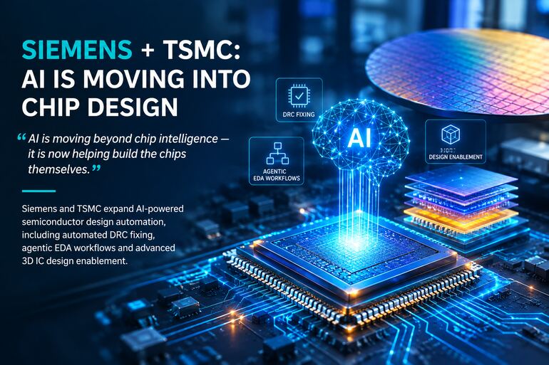
Siemens and TSMC are deepening their collaboration to bring AI-driven automation to chip design and semiconductor manufacturing workflows. Through their longstanding engagement in the TSMC Open Innovation Platform (OIP) ecosystem, the companies are expanding chip design enablement initiatives to help customers navigate rising design complexity, shorten development cycles, and improve engineering productivity.
The collaboration introduces an AI-powered agent that automatically identifies and resolves design rule check (DRC) violations across digital and custom integrated-circuit (IC) design flows. Built on Siemens’ Calibre technology and integrated with Aprisa and Solido software, the solution helps chip design teams reduce repetitive manual work, streamline verification, and move designs to tapeout more quickly.
“Our continued collaboration with TSMC exemplifies Siemens’ commitment to delivering AI-driven automation and advanced semiconductor design capabilities that help customers innovate at the industry’s most advanced process nodes,” said Ankur Gupta, executive vice president, EDA IC Software, Siemens Digital Industries Software. “By combining Siemens’ EDA portfolio with TSMC’s leading process and packaging technologies, we are helping customers achieve new levels of productivity, speed and design confidence.”
“AI presents a significant opportunity to drive productivity and efficiency across increasingly complex semiconductor design workflows,” said Aveek Sarkar, director of the ecosystem and alliance management division at TSMC. “Our collaboration with OIP partners like Siemens focuses on delivering intelligent, trusted automation that empowers engineers to navigate rising design complexity while achieving stringent performance and energy-efficiency targets. By integrating AI into critical stages of the design process, we enable mutual customers to leverage TSMC’s industry-leading processes and advanced packaging technologies to accelerate the expansion of AI innovation.”
Also Read: India Opens New Front in Semiconductor Race: High-Voltage SiC
Advancing AI-powered Semiconductor design
Siemens and TSMC are expanding their collaboration to advance AI-powered semiconductor design through the Fuse EDA AI System and Fuse EDA AI Agent. These technologies enable autonomous, long-running, and self-verifying EDA workflows that can reason through complex, multistep design challenges, coordinate actions across multiple EDA tools, and continuously evaluate and refine results. Enhanced with NVIDIA AI technologies, the Fuse EDA AI Agent delivers greater token efficiency while strengthening reasoning and execution across extended engineering workloads.
A key innovation is an AI-powered DRC-fix workflow that brings together Calibre software, Aprisa AI, and Solido Fuse technologies to identify, analyze, and resolve design-rule violations across digital and custom IC design flows. Building on the Calibre Check Assist capability which provides contextual guidance and relevant design-rule information during DRC debugging, the workflow helps designers diagnose issues faster and resolve them more effectively. The collaboration also extends to agentic custom IC design capabilities powered by Solido Fuse.
In addition, the collaboration supports agentic place-and-route and digital implementation workflows enabled by Aprisa software. By combining domain-aware AI guidance with intelligent automation, these innovations help engineering teams reduce repetitive, time-consuming tasks, accelerate design convergence, and improve productivity across the design journey from initial creation through tapeout.
Supporting TSMC 3DFabric technologies
Siemens and TSMC continue to advance 3D IC design enablement for TSMC 3DFabric technologies. Siemens has expanded Calibre 3DStack Advanced software with multi-machine support for inter-chiplet antenna verification, including support for TSMC-SoIC, TSMC’s wafer-level 3D IC chip-stacking platform. Certification is also underway for chip-on-wafer-on-substrate with local silicon interconnect (CoWoS-L). These enhancements provide the scalability and runtime performance required for increasingly complex 3D IC designs, while joint work has demonstrated performance improvements in the Interface Check Flow for TSMC-SoW.
Siemens’ EDA portfolio, including Solido Simulation Suite software, Calibre xACT software, and Calibre 3DThermal software continues to support collaborative design initiatives with TSMC across advanced 3D IC and multiphysics applications. These efforts encompass silicon photonics as well as other emerging advanced-packaging technologies.
In addition to certification for static and transient thermal analysis of TSMC 3DFabric technologies, Calibre 3DThermal software has been certified for static and transient thermal analysis of TSMC A16 technology and enabled for the system-on-wafer thermal reference flow. Enablement efforts are also underway for the TSMC-COUPE (Compact Universal Photonic Engine) reference flow.
The companies are making continued progress toward comprehensive 3Dblox support, including chip-package co-design workflows developed with major mutual customers. Siemens and TSMC are also collaborating on Aprisa software capabilities for pre-simulation-driven die-to-die (D2D) auto-routing, helping designers develop routing configurations that are intended to meet signal-integrity requirements.
Siemens EDA technologies have also been enabled to support the design, implementation, and verification of TSMC-COUPE features. Joint silicon-photonics development activities include design, implementation, and verification flows using Innovator3D IC Integrator, Calibre 3DStack, Solido Simulation Suite, L-Edit software, and Calibre Interactive. Solido Simulation Suite further supports PAM4 measurements for optical-transceiver interfaces associated with TSMC-COUPE technology, while joint validation of the Calibre 3DThermal solution for TSMC-COUPE remains ongoing.
Enabling advanced process technologies
Siemens and TSMC continue to collaborate on advanced process-node certification and design enablement. Siemens’ Calibre nmDRC, Calibre nmLVS, Calibre xACT, and Calibre PERC technologies have been certified for the TSMC A14 process node, supporting critical verification and reliability requirements for next-generation designs.
Solido Simulation Suite software has also been certified for SPICE accuracy across TSMC N3C, A16, and A14 process technologies, helping enable reliable verification for analog, RF, and memory designs. The collaboration further extends to TSMC’s custom design reference flow, where Siemens technologies provide reliability-aware simulation capabilities for IC aging, real-time self-heating, and safe-operating-area checks. In addition, Solido Design Environment supports advanced variation-aware verification and automated cell optimization.
mPower software has been certified for transistor-level IR-drop and electromigration analysis for TSMC N2P digital and analog designs, as well as N3C analog designs. Siemens and TSMC are also continuing their collaboration on custom design reference flows for electromigration and IR-drop analysis on N2 and N3 technologies. Certification efforts for Aprisa software and mPower analog software on the A14 process are currently underway.
Scaling Ecosystem’s Advanced Node Design Expertise
Siemens Xcelerator Academy provides user-friendly, self-paced, on-demand learning resources for Siemens’ EDA portfolio. The program is now available to TSMC Design Center Alliance partners in addition to mutual customers. Siemens recently released an end-to-end digital implementation flow lab tutorial based on TSMC 5nm process technology through the program, helping broaden access to advanced semiconductor design methodologies.
