



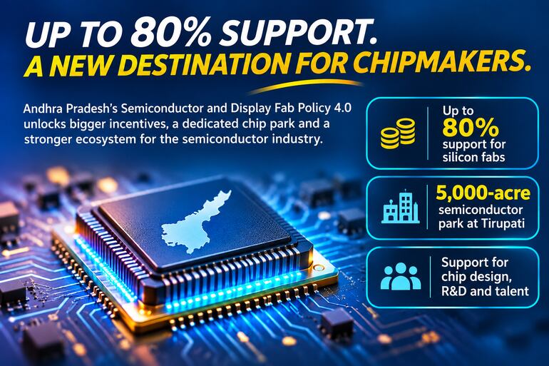
India’s race to become a global semiconductor powerhouse is gaining a new contender. And Andhra Pradesh wants to make its mark on the chip map. With up to 80% combined capital support for eligible silicon fabrication projects and a proposed 5,000-acre semiconductor park in Tirupati, the state is making an ambitious pitch to attract chipmakers and technology investors. But the plan goes beyond building fabrication facilities. From chip design and advanced packaging to machinery, materials, research and talent development, Andhra Pradesh is looking to create an ecosystem that could support multiple stages of the semiconductor value chain.
Announced by Shri Nara Lokesh, Hon’ble Minister for Information Technology, Electronics and Communications, Government of Andhra Pradesh, the Semiconductor and Display Fab Policy 4.0 marks a significant step towards strengthening the state’s technology and manufacturing ambitions. By aligning its incentives with the Centre’s India Semiconductor Mission (ISM) 2.0, the government aims to make the state more attractive to domestic and global investors. “Can this combination of financial incentives, dedicated infrastructure and talent development help Andhra Pradesh emerge as a major destination for semiconductor manufacturing?”
Semiconductor Policy 4.0: Up to 80% Capital Support for Silicon Fabs
One of the biggest highlights of the revized Semiconductor Policy is the enhanced capital assistance available to eligible manufacturing projects.
Under the framework, Andhra Pradesh will match 100% of the Centre’s capital support for specified semiconductor projects. Eligible silicon fabrication units can receive combined assistance of up to 80% of their eligible capital expenditure, comprising 40% from the Centre and 40% from the state.
The incentives also cover several other segments of the semiconductor industry:
- Up to 70% combined support: Compound semiconductor, photonics, sensor, discrete and display fabs, along with advanced packaging units.
- Up to 50% support: Legacy packaging units.
- Up to 48% combined capital support: Semiconductor machinery and materials manufacturing, including 30% central assistance and an additional 18% from the state.
The state has positioned these incentives as a way to improve its competitiveness as an investment destination for semiconductor companies.
5,000-Acre Semiconductor Park Planned in Tirupati
Beyond financial incentives, infrastructure is central to Andhra Pradesh’s semiconductor strategy. The government plans to develop a dedicated 5,000-acre semiconductor park in Tirupati, with the objective of creating a manufacturing and supplier cluster covering the industry’s wider value chain.
The proposed park is expected to offer developed industrial land, shared cleanrooms, reliable high-voltage power with redundancy, ultrapure water, natural gas and specialty gases. It will also include effluent treatment and water recycling facilities, testing laboratories, logistics infrastructure, research facilities and training centres.
The park is planned to operate through a public-private partnership structure with an investor-led board. By bringing critical infrastructure and supporting services together, Andhra Pradesh aims to make it easier for semiconductor manufacturers and allied businesses to establish operations.
Chip Design Startups and Semiconductor Equipment Also Get Support
The revized Semiconductor Policy goes beyond fabrication facilities to support chip design companies, startups and manufacturers of semiconductor machinery and materials.
Commercial chip-design startups can receive combined seed funding of up to ₹22.5 crores, including up to ₹7.5 crores from the state. Under the deployment-linked incentive, the state will add 4.5% of net sales to the Centre’s 9% support, taking the combined incentive to 13.5%, subject to prescribed ceilings.
For semiconductor machinery and materials manufacturing, the state will provide an additional 18% of capital cost over the Centre’s 30% assistance, taking the combined capital support to 48%.
The policy covers 10 categories across six pillars: design, machines and materials, fabrication, packaging, research and development, and talent. This broader coverage is intended to encourage investment across multiple stages of semiconductor production rather than concentrating only on chip fabrication.
Semiconductor Policy Focuses on Research and Talent Development
Building a semiconductor industry requires more than factories and investment. Skilled professionals, research capabilities and access to technology are equally important.
To strengthen this ecosystem, Andhra Pradesh plans to establish the AP Semiconductor Research and Innovation Centre (AP-SRIC), which will initially operate from IIT Tirupati. Photonics has been identified as its first area of focus. The centre is expected to support research, prototyping, testing, technology development and industry collaboration.
The state also plans to establish an AP Semiconductor Training and Capacity Building Centre within the proposed semiconductor park. Its training programmes will be developed in collaboration with industry and universities.
Companies can avail themselves of a training subsidy of ₹10,000 per trainee per month for a period of six months. The policy also provides state support covering 25% of eligible costs for research and talent development projects, with total assistance from the Centre and state capped at 75% of the project cost.
Single-Window Support for Semiconductor Investors
To simplify the investment process, the policy proposes the AP Semiconductor Growth and Innovation Council (APSGIC) as a single point of contact for investors.
The council will have an Oversight Council chaired by the Chief Minister and a CEO-led Apex Committee comprising experts. It is expected to help appraise projects, recommend state incentives and coordinate clearances, land allocation, power and water requirements, as well as engagement with the Centre.
The policy also provides for customized incentive packages for mega projects involving investments between ₹1,000 crore and ₹5,000 crore, and ultra-mega projects exceeding ₹5,000 crore. These packages will be considered on a case-by-case basis.
The amended policy will remain valid for five years or until it is replaced by a new policy. The government will also issue separate operational guidelines covering eligibility, project appraisal and the disbursement of incentives.
Can Andhra Pradesh Become a Major Semiconductor Manufacturing Hub?
With enhanced capital incentives, a proposed 5,000-acre semiconductor park and dedicated research and training facilities, Andhra Pradesh is seeking to strengthen its position in India’s semiconductor landscape.
The revized Semiconductor Policy 4.0 covers several critical areas, from chip design and fabrication to packaging, equipment, research and workforce development. Its wider ambition is to attract investments while building the supporting ecosystem needed to manufacture and develop semiconductor technologies within the country.
However, the success of this strategy will depend on attracting committed investors, developing the proposed infrastructure, implementing the incentive framework and building a skilled workforce.
As India works to strengthen its domestic semiconductor capabilities and diversify global supply chains, Andhra Pradesh’s latest policy amendment represents an important step in its effort to become a destination for the next phase of chip manufacturing and innovation.
