



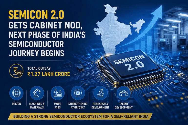
The Union Cabinet chaired by Prime Minister Shri Narendra Modi has approved Semicon 2.0, a new phase of India’s semiconductor mission with a total budget outlay of ₹1.27 lakh crores. The initiative aims to strengthen the country’s semiconductor design and manufacturing ecosystem while building on the progress made under the first phase of the programme.
The government said Semicon 2.0 is designed to provide long-term support to India’s semiconductor industry and position the country as a global hub for chip design, manufacturing, research and innovation.
What is Semicon 2.0?
Semicon 2.0 is the next phase of India’s semiconductor development programme. It expands the scope of the earlier initiative by supporting not only chip manufacturing but also design, research, advanced packaging, materials, equipment manufacturing and talent development.
The programme is expected to help India reduce its dependence on imported semiconductors while encouraging domestic production of chips used in smartphones, electric vehicles, consumer electronics, telecom equipment, defence systems and Artificial Intelligence (AI) applications.
Also Read: https://webnewsaddiction.com/tata-semiconductor-assam-incentives/
Six Key Focus Areas of Semicon 2.0
1. Boosting Chip Design
The government plans to strengthen India’s semiconductor design ecosystem by encouraging startups and companies to develop chip intellectual property (IP), advanced chip designs and complete semiconductor systems. According to the government, more than 105 startups are already working on semiconductor chip designs under the earlier programme. The next phase aims to build on this momentum.
2. Supporting Machines and Raw Materials
Semiconductor manufacturing depends on highly specialized machinery, chemicals, gases and materials. Under Semicon 2.0, companies manufacturing these critical components in India will receive government support. This is expected to strengthen the domestic semiconductor supply chain and encourage precision manufacturing.
3. Encouraging More Semiconductor Fabs
The government also wants to attract more companies to establish semiconductor fabrication facilities (fabs) in India.
These may include:
- Silicon fabs
- Compound semiconductor fabs
- Display fabs
- Discrete component manufacturing units
India’s first semiconductor fab is expected to become operational in 2028, and the government hopes additional investments will follow.
4. Expanding Chip Packaging Industry
Semicon 2.0 will also focus on strengthening India’s ATMP (Assembly, Testing, Marking and Packaging) and OSAT (Outsourced Semiconductor Assembly and Test) ecosystem. These facilities package and test semiconductor chips before they reach electronics manufacturers. The government believes India can emerge as an alternative destination for advanced semiconductor packaging.
5. Increasing Research and Development
Currently, India’s semiconductor manufacturing efforts are focused on technologies ranging from 28nm to 110nm process nodes. The new programme aims to support research into more advanced semiconductor technologies through collaborations with leading research institutions in India and abroad.
6. Developing Skilled Talent
The government will continue investing in semiconductor education and workforce development.
So far:
- 315 universities have been involved in semiconductor training.
- Around 68,000 students have received training using industry-standard Electronic Design Automation (EDA) tools.
The next phase will expand training in chip design, semiconductor fabrication, clean-room operations and related technologies.
Also Read: https://webnewsaddiction.com/cg-semi-osat-facility-explained/
How Semicon 2.0 Could Shape India’s Tech Future
Semiconductors are often called the “brains” of modern electronic devices because they power everything from smartphones and laptops to electric vehicles, medical equipment, telecom networks and defence systems. Countries around the world are investing heavily in semiconductor manufacturing to reduce dependence on global supply chains and improve technological self-reliance. With Semicon 2.0, India aims to strengthen its position in this strategically important industry while creating new investment opportunities, generating skilled jobs and supporting long-term economic growth.
Progress Under Semicon 1.0
The government highlighted significant progress made under the first phase of the India Semiconductor Mission.
Manufacturing
- 12 semiconductor manufacturing units have been approved.
- Total investment exceeds ₹1.64 lakh crores.
These include:
- One silicon fabrication plant
- One silicon carbide fab
- One Gallium Nitride (GaN) Micro LED display fab
- Nine semiconductor packaging units
Commercial production has already started at Micron, Kaynes and CG Semi, while another facility is expected to begin operations in 2026.
Design Ecosystem
The government has approved 24 semiconductor design projects from startups and MSMEs for financial assistance. In addition, 105 startups and MSMEs have received access to advanced Electronic Design Automation (EDA) software for designing semiconductor chips used in applications such as:
- Artificial Intelligence (AI)
- Internet of Things (IoT)
- Satellite communication
- Drones
- Smart meters
- Telecom equipment
- Surveillance systems
- LED drivers
Many of these projects are currently under development and are expected to move towards commercial deployment after successful prototyping.
Looking Ahead
With the launch of Semicon 2.0, the government is seeking to create a complete semiconductor ecosystem covering design, manufacturing, packaging, research and workforce development.
If implemented successfully, the programme could help India become an important player in the global semiconductor industry while strengthening domestic manufacturing and supporting future technologies across sectors ranging from electronics and automobiles to defence and artificial intelligence.

1 Comment
Pingback: Rohde & Schwarz Showcases Test Solutions at EuMW 2026