



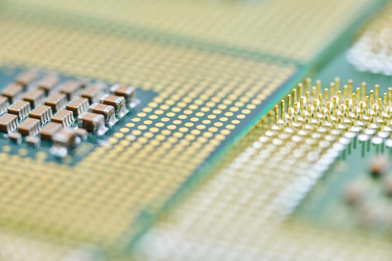
When people talk about semiconductors, the conversation almost always revolves around chip fabrication, the highly sophisticated process of manufacturing semiconductor wafers. Yet, one equally critical stage often receives far less attention: chip packaging and testing. The recent inauguration of CG Semi’s Outsourced Semiconductor Assembly and Test (OSAT) facility in Sanand, Gujarat brings this often-overlooked stage into focus. More than another manufacturing milestone, it reflects India’s growing efforts to build a complete semiconductor ecosystem.
The Role of Chip Packaging in Semiconductor Manufacturing
A semiconductor isn’t ready for use immediately after it’s manufactured. Before it powers a smartphone, electric vehicle, data centre or AI application, it must be assembled, packaged and rigorously tested to ensure reliability and performance.
This is where OSAT facilities come in. These facilities transform fabricated chips into finished semiconductor components that can be integrated into thousands of electronic products. In many ways, packaging and testing bridge the gap between chip manufacturing and real-world applications.
Building an Ecosystem, Not Just Factories
The global semiconductor industry isn’t built around a single manufacturing plant. It thrives on interconnected ecosystems that bring together chip designers, fabrication units, packaging facilities, equipment suppliers, specialized chemical manufacturers, logistics providers, testing laboratories and a highly skilled workforce. India’s semiconductor ambitions are increasingly moving in this direction.
Countries that dominate semiconductor manufacturing today developed these ecosystems over decades through continuous investment in infrastructure, research, workforce development and supply chain integration. Rather than focusing solely on manufacturing capacity, they created environments where every stage of semiconductor production could operate efficiently. For India, developing similar capabilities across the value chain will be essential to improving competitiveness and reducing dependence on overseas manufacturing and testing services.
The commissioning of another commercial OSAT facility adds an important capability to the country’s growing semiconductor infrastructure, complementing ongoing investments across electronics manufacturing and semiconductor production.
Strengthening India’s Semiconductor Value Chain
While the Sanand facility was inaugurated by Prime Minister Shri Narendra Modi as part of India’s semiconductor push, its significance extends beyond the ceremony itself.
The development reflects a broader national strategy to strengthen domestic capabilities across the semiconductor value chain, from design and manufacturing to packaging and testing. Rather than relying entirely on overseas partners for critical stages of production, India is gradually expanding its role in the global semiconductor supply chain.
As more semiconductor-related investments enter the country, the availability of domestic packaging and testing capabilities can help support a broader manufacturing ecosystem while creating opportunities for technology transfer, supplier development and skilled employment.
The Significance of Chip Packaging
Demand for semiconductors continues to grow as industries adopt Artificial Intelligence, Electric Mobility, Advanced Consumer Electronics, Industrial Automation and Connected Devices. Meeting this demand requires more than chip fabrication alone. Packaging and testing have become increasingly sophisticated, influencing performance, power efficiency, reliability and the integration of advanced technologies.
Modern semiconductor packaging is no longer just about protecting a chip. Advanced packaging technologies enable greater computing performance, improved thermal management and higher levels of integration that are becoming increasingly important for AI processors, automotive electronics and high-performance computing applications. As semiconductor technologies evolve, packaging is emerging as a strategic capability that contributes directly to product innovation.
As a result, OSAT facilities are no longer viewed as supporting infrastructure. They are an essential part of modern semiconductor manufacturing.
What’s Next for India’s Semiconductor Ecosystem
India’s semiconductor ecosystem is still developing and building global competitiveness will require sustained investment, skilled talent, supply chain resilience and continued policy support. The CG Semi OSAT facility is one step in that direction. It may not transform the industry overnight, but it strengthens an area that has often received less public attention despite being vital to the semiconductor value chain.
As India works towards becoming a larger player in global electronics manufacturing, the conversation is gradually shifting from simply making more devices to building the infrastructure that powers them.
That makes chip packaging more than just another stage in production. It is becoming one of the key building blocks of India’s semiconductor ecosystem.
