



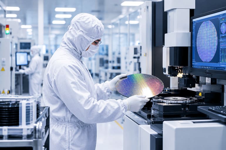
HCLTech, a leading global technology company, has inaugurated a new Advanced Semiconductor Lab in Bengaluru. Built with an investment of ₹185 crore, the facility underscores HCLTech’s commitment to advancing semiconductor innovation and shortening time-to-market for its global clients, while establishing the company as a pioneer among service providers offering integrated semiconductor testing capabilities.
Drawing on two decades of semiconductor expertise, the 40,000 sq ft lab includes 25,000 sq ft of Class 10K and Class 1K cleanrooms and provides end-to-end post-silicon engineering, advanced testing, and failure analysis. Equipped with state-of-the-art tools from Teradyne, Advantest, Keysight, Tektronix, and Thermo Fisher Scientific Inc., the facility supports R&D, pre-production, and production qualification, helping customers achieve faster turnaround, higher quality, and reduced complexity.
Also Read: Torrent Green Energy Completes One of Maharashtra’s Biggest Decentralized Solar Projects
Aligned with HCLTech’s Spec2Parts business model, the lab offers a unified platform for electrical validation, automated testing, qualification, and failure analysis, streamlining the path from design specifications to finished semiconductor parts.
By addressing critical gaps in India’s semiconductor ecosystem, the lab enables HCLTech to deliver faster and more comprehensive solutions. Customers gain access to cutting-edge facilities and highly skilled teams, fostering greater innovation and efficiency for both clients and the broader industry.
Also Read: Point S Equips Future Leaders to Manage Workshop Growth in a Changing Market
“The inauguration of our Advanced Semiconductor Lab in Bengaluru is a proud milestone for HCLTech and reinforces India’s growing leadership in semiconductor innovation. This facility reflects our deep commitment to investing in high-end engineering capabilities. We are excited to contribute to the country’s vision of becoming a global hub for advanced technology,” said Hari Sadarahalli, Corporate Vice President and Global Head, Engineering and R&D Services at HCLTech.
HCLTech’s facility is set to achieve global certifications, including ISO 17025, ISO 9001, AS 9100 (Mil-Aero) and ISO 13485 (Medical). Its cleanroom houses the latest ATE testers, probes, qualification chambers and advanced failure analysis tools, including optical and electron microscopy and focused ion beam (FIB) systems.
Serving both domestic and international markets, the lab is a cornerstone of HCLTech’s global strategy to deliver innovative, high-quality semiconductor solutions and to strengthen India’s leadership in the sector.

2 Comments
Pingback: Maharashtra’s Next Big Power Play Could Be Nuclear
Pingback: TI Showcases EV Semiconductor Innovations